inside the sm: warps, partitions, and how gpus schedule work
a deep dive into gpu streaming multiprocessors: sm partitions, warp execution, the simt model, thread divergence, and nvlink interconnect - the hardware mechanics behind gpu compute.
In the last post I covered the performance metrics - bandwidth, TFLOPS, precision, tensor cores. Those are the what: what a GPU can do on paper. This post is about the how: how the GPU actually organizes and executes work at the hardware level.
We're going inside the Streaming Multiprocessor (SM) - the execution engine that does all the real work - and looking at how NVIDIA structures its hardware from the silicon die up through warps, partitions, and scheduling.
GPU Chip vs GPU Product
Before we go inside the SM, let's clarify something that tripped me up early: a GPU chip and a GPU product are not the same thing.
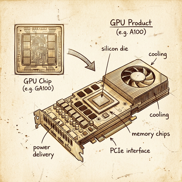
The GPU chip is a piece of silicon - the die itself. It contains the SMs, the L2 cache, the memory controllers, and the interconnect fabric. That's it. It has a codename like GA100, GH100, or GV100.
The GPU product is everything else wrapped around that chip to make it usable: the PCB, the HBM/GDDR memory chips soldered around the die, the power delivery (VRMs), the cooling solution (heatsink, fan, or vapor chamber), and the interface connector (PCIe or SXM).
NVIDIA's chip naming convention encodes the architecture:
| Prefix | Architecture | Example Chip | Example Product |
|---|---|---|---|
| GF | Fermi | GF100 | Tesla X2070 |
| GK | Kepler | GK210 | K80 |
| GM | Maxwell | GM200 | M60 |
| GP | Pascal | GP100 | P100 |
| GV | Volta | GV100 | V100 |
| GA | Ampere | GA100 | A100 |
| GH | Hopper | GH100 | H100 |
| AD | Ada Lovelace | AD107 | L4 |
Pattern: G + first letter(s) of architecture + chip variant number. Once you see it, you can decode any NVIDIA chip name instantly.
Why does this matter? Because when you read a whitepaper that says "GA100 has 128 SMs," that's the full chip. The A100 product ships with 108 SMs enabled - NVIDIA disables some for yield (manufacturing defects) and for product segmentation. The chip and the product have different specs.
NVIDIA's Product Taxonomy
NVIDIA sells GPUs into very different markets, and the product line tells you which one:
| Product Line | Market | Example | Cooling |
|---|---|---|---|
| Tegra | Mobile / embedded | Nintendo Switch, Jetson | Passive / thermal solution |
| GeForce | Consumer gaming | RTX 3090, RTX 4090 | Fan(s) |
| Quadro / RTX Pro | Professional workstations | RTX A4000, RTX A6000 | Blower fan |
| Tesla / Data Center | HPC and AI | V100, A100, H100 | No fan (server airflow) |
The cooling distinction is a good tell. If a GPU product has no fan, it's designed for data center racks where the server chassis provides airflow. If it has fans, it's designed for workstations or consumer PCs. This is a practical detail that matters when you're racking hardware - a fanless Tesla/HPC card will thermal throttle immediately on an open bench.
NVIDIA has been phasing out the "Tesla" branding (to avoid confusion with the car company) and now refers to data center GPUs by their architecture name directly: A100, H100, etc.
Inside the SM: Partitions All the Way Down
Now let's get into the core of the GPU: the Streaming Multiprocessor. If you saw the first post in this series, you know the SM is where all compute happens. But an SM isn't a single monolithic unit - it's subdivided into partitions.
Take the Volta GV100 SM as an example. It's split into 4 partitions, and each partition is essentially a self-contained processing unit with its own:
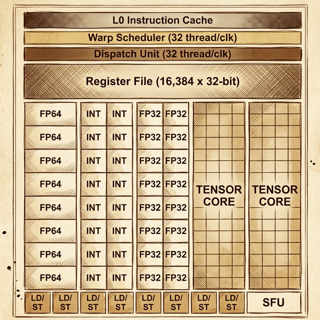
From top to bottom inside each partition:
- L0 Instruction Cache - stores decoded instructions so the partition doesn't have to fetch from the SM-level L1 cache on every cycle
- Warp Scheduler - manages warps assigned to this partition and decides which warp's instruction to issue each cycle (32 threads per clock)
- Dispatch Unit - routes the selected instruction to the correct execution units (32 threads per clock)
- Register File (16,384 × 32-bit) - fast local storage for thread state. Each thread gets its own registers; the register file is partitioned across all active threads
- Compute Units:
- 8 × FP64 cores - double-precision floating-point
- 16 × INT cores - integer operations (two columns of 8)
- 16 × FP32 cores - single-precision floating-point (two columns of 8)
- 2 × Tensor Cores - matrix multiply-accumulate for deep learning
- 8 × LD/ST units - Load/Store units for memory operations
- 1 × SFU - Special Function Unit for transcendental math (sin, cos, exp, sqrt)
So the full Volta SM has 4 of these partitions, which means the entire SM contains:
- 4 warp schedulers (one per partition)
- 64 FP32 cores (16 per partition × 4)
- 32 FP64 cores (8 per partition × 4)
- 64 INT cores (16 per partition × 4)
- 8 tensor cores (2 per partition × 4)
- 32 LD/ST units (8 per partition × 4)
- 4 SFUs (1 per partition × 4)
Above all 4 partitions sits the shared L1 Data Cache / Shared Memory (128 KB on Volta) and the L1 Instruction Cache. These are SM-level resources that all partitions share.
Warps: 32 Threads in Lockstep
This is the concept that makes GPU execution different from anything on a CPU: the warp.
A warp is a group of 32 threads that execute the same instruction at the same time, each on different data. This is NVIDIA's implementation of SIMT - Single Instruction, Multiple Threads. It's conceptually similar to SIMD (Single Instruction, Multiple Data) on CPUs, but with a key difference: each thread has its own program counter and register state, so threads can diverge (take different branches), though at a performance cost.
Here's how threads become warps:
- You launch a CUDA kernel with some number of thread blocks (also called "blocks")
- Each thread block is assigned to an SM
- The SM subdivides each block into warps of 32 threads
- Each warp is assigned to one of the SM's partitions
- The partition's warp scheduler manages that warp's execution
The math is simple:
warps_per_block = ceil(block_size / 32)
If your block has 256 threads: 256 / 32 = 8 warps. If your block has 100 threads: ceil(100 / 32) = 4 warps - but that last warp only has 4 active threads, and the other 28 are idle. Those idle threads still consume resources. This is why choosing a block size that's a multiple of 32 is one of the most basic CUDA optimization rules.
Warp Scheduling: Hiding Latency
Here's the part that surprised me: a single SM partition doesn't just run one warp. It has many warps assigned to it simultaneously, and the warp scheduler switches between them every cycle.
Why? Because GPU memory operations are slow - a load from global memory can take hundreds of clock cycles. Instead of stalling and waiting (like a CPU would), the warp scheduler simply switches to a different warp that's ready to execute. By the time it cycles back to the original warp, the memory operation has (hopefully) completed.
This is why GPUs need so many threads: not because each thread does a lot of work, but because massive thread counts hide memory latency. The more warps the scheduler has to choose from, the less likely it is to stall. This is called latency hiding through occupancy.
The Volta SM, for example, can have up to 64 warps resident simultaneously (2,048 threads). That's 16 warps per partition available to the warp scheduler at any time.
Thread Divergence: The Performance Killer
Remember that all 32 threads in a warp execute the same instruction each cycle. So what happens when threads in a warp hit an if/else branch and some go left while others go right?
The hardware handles it, but serially. First, the threads taking the if branch execute while the others are masked (disabled). Then the threads taking the else branch execute while the first group is masked. The warp executes both paths, taking the time of both.
This is thread divergence, and it's one of the most common performance pitfalls in CUDA programming. Code that causes heavy divergence within a warp can effectively halve throughput (or worse, with nested branches). The ideal case is all 32 threads taking the same branch - no divergence, no performance penalty.
The Full Picture: SM → Partitions → Warps → Cores
Let's trace the execution hierarchy from top to bottom:
- GPU chip has N SMs (e.g., GA100 = 128 SMs, A100 product = 108 SMs)
- Each SM is split into partitions (4 on Volta/Ampere)
- Each partition has a warp scheduler managing multiple resident warps
- Each warp is 32 threads executing the same instruction
- Each thread executes on a single core (FP32, FP64, INT, or tensor)
The warp scheduler in each partition selects one ready warp per cycle and dispatches its instruction to the 16 FP32 cores (or 8 FP64 cores, etc). Since a warp has 32 threads but a Volta partition only has 16 FP32 cores, a single FP32 warp instruction takes 2 cycles to dispatch all 32 threads (16 per cycle). This is why you'll sometimes see references to "sub-warp" execution in NVIDIA documentation.
NVLink: Connecting Multiple GPUs
A single GPU - no matter how powerful - has limits. For large-scale ML training, you need multiple GPUs working together. This is where NVLink comes in.
NVLink is NVIDIA's proprietary high-speed GPU-to-GPU interconnect. It's fundamentally different from PCIe:
| Feature | PCIe Gen4 ×16 | NVLink 3.0 (A100) | NVLink 4.0 (H100) |
|---|---|---|---|
| Bandwidth per link | 32 GB/s each way | 25 GB/s per link | 25 GB/s per link |
| Total links | 1 | 12 | 18 |
| Total bandwidth | 64 GB/s bidirectional | 600 GB/s | 900 GB/s |
The A100's NVLink delivers 600 GB/s of total bandwidth between GPUs - almost 10× what PCIe provides. The H100 pushes this to 900 GB/s. This matters because multi-GPU ML training involves constant communication between GPUs: gradient synchronization, model parameter updates, and data shuffling.
NVIDIA packages NVLink-connected GPUs into purpose-built systems:
- DGX A100: 8× A100 GPUs connected via NVLink and NVSwitch (a 6-switch fabric that gives every GPU full-bandwidth access to every other GPU)
- DGX H100: 8× H100 GPUs with 4th-gen NVLink and NVSwitch
- HGX: the server board (without the chassis) used by cloud providers like AWS, Azure, and GCP in their GPU instances
If you've ever wondered why cloud GPU instances are so expensive, this is part of the answer: you're not just paying for the GPUs, you're paying for the NVLink fabric that connects them. A DGX H100 system costs around $300,000–$500,000.
Why This Architecture Matters for Software
Understanding the SM hierarchy directly impacts how you write and optimize CUDA code:
- Block size should be a multiple of 32 - anything else wastes threads in the last warp
- Maximize occupancy - more resident warps per SM means better latency hiding. Don't use too many registers per thread or too much shared memory, because these are finite per-SM resources that limit how many warps can be resident
- Avoid thread divergence - keep threads within each warp taking the same branch. If divergence is unavoidable, restructure your data so that threads with similar behavior end up in the same warp
- Balance compute and memory - the LD/ST units and memory hierarchy are separate from the compute cores. A kernel that's purely memory-bound will leave the FP32 cores idle; one that's purely compute-bound will stall on memory
This maps directly to the profiling tools we'll discuss in the next post - NVIDIA's Nsight Compute can show you exactly how many warps are active, how much divergence is happening, and whether your SM utilization is compute-bound or memory-bound.
What's Next
We've gone from the silicon die through SMs, partitions, warp schedulers, and all the way down to individual cores. In the next post, we'll zoom out to the software layer: the CUDA toolkit - the compiler (nvcc), the libraries (cuBLAS, cuDNN), the host-device programming model, and the full execution pipeline from your .cu source file to actual GPU execution.
The hardware is the machine. The toolkit is how you talk to it.
Resources
backlinks 0
see also
get the rest of the series.
i'll send each new essay the morning it ships. nothing else.